When designing the CPC and its firmware, Amstrad and Locomotive Software planned for a way to expand the OS by adding extra ROMs. This allowed integration of the floppy controller ROM in a mostly transparent and user-friendly way, but it also allows much more. ROMs can register commands known as RSX (Resident System Extensions) and allow to have various tools immediately available at boot.
Initially, the ROMs were actually ROMs. You could either buy devices that came with a single expansion ROM inside them (the Hacker is an example of that). But a somewhat popular expansion for the CPC is to add a "ROM Board", which is a device that connects to the expansion port and allows to add extra ROMs. There are some commercial ones as well as DIY projects, of which the Inicron ROMBox is one of the most known.
However, the use of ROM is a bit unconvenient. Programming ROMs require dedicated hardware, making updates annoying, and, maybe more importantly, making development of such ROMs quite difficult. The first device to solve this was Ram7's RAMCard. Instead of ROM, it used a battery-backed static RAM that would keep its content when the CPC was turned off. An hardware switch allows to enable write access to the "ROM" space and update the software stored there very easily. For full details, check our page about the RAMCard.
The RAMCard enabled easy development of many ROM-based tools for the CPC, being a very popular expansion for many users. However, it came with its own problems. The battery could run out, and plugging, unplugging or moving the RAMCard around (when travelling to a CPC users meeting, for example), would often lead to corrupt ROMs and an unbootable system.
The next step was to use Flash memory instead. Flash memory does not need a battery backup, and the data is secured by a specific access sequence to avoid accidental writes. This makes moving the device around a lot more secure. This idea was implemented by Bryce in the MegaFlash board. The FlashGordon is largely a clone of the MegaFlash, with the following changes:
The FlashGordon hardware went through several iterations:
FlashGordon comes pre-loaded with ROMAN in ROM slot 15. ROMAN includes a ROM booster that will automatically initialize ROMs 31 to 16 at boot (the CPC firmware only initializes ROMs 15 to 0). ROMAN allows program ROMs in the different slots, temporarily disable them, save them back to disk, and list the RSXs provided by each installed ROM.
Download ROMAN 2.0 (dsk and user manual)PulkoMandy manages the manufacturing and shipping of the cards. After an initial batch of 40 cards in 2012, the card was redesigned a bit in 2020 to use smaller components and be easier to assemble. Contact me if you want one. The price is set to 25€ including wordwide shipping. Please contact me before sending a payment, as I'm doing this in my free time between many other projects and things, and there could be long delays. I don't want to be owing you money for years.
The Kicad project is available on my Git repository.
git clone https://pulkomandy.tk/gerrit/avrstuff
FlashGordon connects to the expansion port using an adapter cable. On the computer side, you need either an HE-902 edge connector (for Amstrad CPC) or a Centronics connector (Amstrad Plus, Schneider CPC). On the other side, you need a female HE10 connector. Try to keep the cable as short as possible (no more than 20cm), else you can get into some problems with the system reliability.
Take the board with the components facing up, and the HE10 connector towards the computer expansion port. When holding the board this way, the connection cable is wired straight. Pin 1 is on the left, as indicated by the arrow on the board. Notice that the 50-pin HE10 connector is wired backwards (pin 1 should be on the right to match the standard), but this allows for easier connection with the CPC.
Alternatively, you can connect the board on a MotherX4 in the usual orientation (components side facing you).
Power up the computer. It should boot at usual, but show the welcome message of the ROM manager. If something does not go as expected, unplug everything and start over. The hardware is tested before shipping, so problems come from either your cable, a dirty expansion port, or something plugged the wrong way.
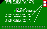
There are 2 jumpers and a push switch on the board. The push switch enables write mode, and the jumpers allow configuration of ROMs 0 and 7 as well as a global disable mode.
The write switch is used to completely prevent write access to the Flash memory. When the light is on, write is allowed. When the light is off, write is not allowed. Note that due to the use of flash memory, normal software should not accidentally write to the ROMs, even if you leave the switch on. It is safe to leave it enabled all the time.
Warning: because of an hardware design limitation, when in write mode, the flash memory will see anything written to both the 8000-BFFF and the C000-FFFF RAM areas. This could lead to unexpected results.
Note: the Flash chip used requires a special programming algorithm, which makes it incompatible with the Megaflash and Ramcard software in write mode.
The two jumpers are used to control the state of ROMs 0 and 7. These need special care because they are the internal ROMs in the computer. ROM 0 is the BASIC, and ROM 7 is the AMSDOS. Most of the time, you want to keep these useable. This is the factory setting: both jumpers are placed near the connector, so the internal ROMs are used.
The top jumper is for ROM 0, and the bottom one is for ROM 7.
If you completely remove the ROM 0 jumper, all the ROMs will be disabled. This is useful if you messed up one of the ROM and it makes the computer unable to boot with the ROMs enabled. Once booted, you can load the recovery program and then enable the board again when it asks you to turn the write switch on. This is the only case where you're allowed to change the jumper settings while the CPC is running.
There is a write switch in the middle and 4 DIP switches at the top of the card.
The write switch is used to completely prevent write access to the Flash memory. When the light is on, write is allowed. When the light is off, write is not allowed. Note that due to the use of flash memory, normal software should not accidentally write to the ROMs, even if you leave the switch on. It is safe to leave it enabled all the time.
This version of the card provides full decoding, so the problem mentioned above about addresses 8000-BFFF does not exist anymore.
DIP switch number 2 is used to enable (right) or disable (left) all ROMs.
Switches number 3 and 4 are used to disable (right) or enable (left) ROMs 0 and 7. When disabled, the CPC internal ROMs are used. When enabled, the ROM flashed in the MegaFlash is used.
On CPC 6128 and DDI-1, the internal ROM 7 can't be cleanly disabled (it works on some machines, but it means the internal ROM and the flash chip both use the memory bus at the same time, and it happens that the flash chip is stronger in this fight. But it could eventually damage the hardware), so you should always leave the ROM 7 jumper down. On Plus and machines without disk drives, you can enable it. ROM 0 can always be overloaded, but remember that you will not boot to the BASIC in that case (the Hacker ROM is a popular replacement ROM 0, for example).
If you are interested in making your own ROM expansion for the CPC, the information below might be useful. Or if you are just curious how this all works. This section will walk you through the schematics (complete schematics and PCB design files are available in my "avrstuff" repository).
git clone https://pulkomandy.tk/gerrit/avrstuff
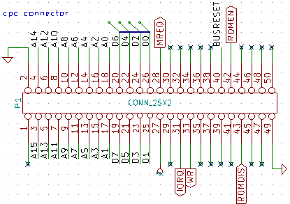
The expansion port is mostly signals coming directly from the Z80 CPU, but there are also a few additional things.
These are the pins D0 to D7 and A0 to A15.
The data bus is 8 bits and is used by the Z80 to send and receive data. Whenever any memory or I/O device is read or written, these 8 pins are used to carry the value around.
The address bus is 16 bits and allows to select which memory address or which device is being used.
Several other signals ensure cooperation and synchronization between the different devices on the bus (expansion cards, but also internal RAM, ROM and peripherals in the CPC). Only a few of them are used in the FlashGordon, here they are:
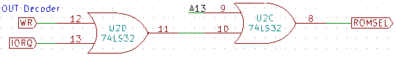
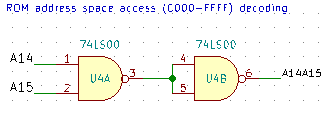
So, to start with, we need to know which ROM is currently active. The ROM number selection is done with an out to register DF00, but in fact, any address with bit 13 = 0 will do.
We need to check 2 things to detect this:
We can check this easily with an OR gate (part number 74HCT32), which conveniently outputs 0 if all inputs are 0 at the same time, and 1 otherwise.
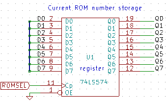
When we detect this, we know that the data bus is currently giving us the ROM number to activate. We don't need it immediately, but we need to remember it for later when ROM access happens. So, we have to store it somewhere. Conveniently, the 74HCT574 chip does just that: when an input pin is 0, it stores an 8bit value. It then remembers it until a new one is written. We note this rom number bits Q0 to Q7 in the schematics.
First of all, we need to know if the CPC is trying to access a ROM at all. Normally, we would use the ROMEN pin on the expansion port for this, but there is a problem: since we use flash memory, we want to also detect writes to the ROM, so they can be reprogrammed, and ROMEN doesn't work for this. So, we need to perform some checking on our own.
The first thing is to decide if the access is in the ROM area. On the CPC, this is C000 to FFFF (other parts of the memory space are used for RAM, firmware ROM, and the ASIC on Plus machines).
We can detect this address range by looking at A15 and A14, if they are both 1, it's an access in the ROM area.
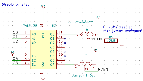
Two ROMs are already built into the CPC: ROM 0 and 7. ROM 0 can be disabled (using the ROMDIS pin), but ROM 7 usually can't (except on Plus machines). So, the FlashGordon provides a way to skip either of these. This is done using bits Q0 to Q3 of the ROM number. If Q3 and Q4 are 0, and Q0-Q2 are all 0 or all 1, one of these ROMs is being accessed. We use a 74HCT138 chip which can check both cases at the same time and put one of its output pins (O0 or O7) to 0 in case of a match.
Then there are the two jumpers which allow to enable these ROMs (by not using the output of this check) or disable them (by using the output). This results in the signals R0EN and R7EN (ROM 0 enable, ROM 7 enable).
There is an additional trick here: when the jumper for ROM 0 is left unconnected, there is a pull down resistor (R5). This forces the signal to 0, and the result is always disabling all ROMs. This is useful if the ROM content is corrupt or you flashed a broken ROM, making it impossible to boot with the FlashGordon connected to the CPC. You can then boot the CPC with ROMs disabled, run a ROM flashing tool, and then put the jumper back and reflash your ROM with a fixed version.
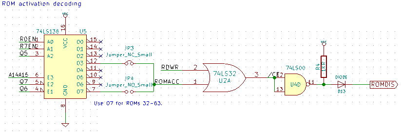
We are not done yet: we need to check that the ROM access was in our range at all by checking bits Q5-Q7 which were missing from the previous comparison. A solder point on the FlashGordon allows to easily modify it to expect Q5=1, in which case it would provide ROMs 32 to 63 instead of 0 to 31.
At this stage, we also put in the check for A14 and A15 mentionned earlier, and the RDWR signal (more on that later). The result of all this is a CE signal (Chip Enable) that goes low whenever there is an access to one of our active ROMs. When that is the case, we also have to tell the CPC internal ROMs to not handle the access (the BASIC ROM in the CPC acts as a backup and always activates if no other ROM is active). This is done using the ROMDIS pin. Unlike CE, it has to go to 1 when we handle a ROM access. Moreover, we need to use a diode, because we only want to force it to 1, and otherwise let other devices on the expansion bus decide if they want to handle other ROM accesses.
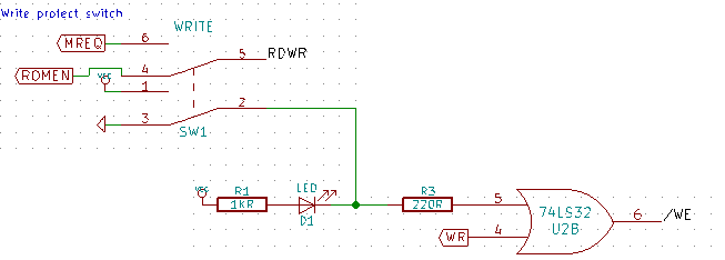
While it is not really needed on the FlashGordon, there is a write protection switch. Accidental writes should not be a problem, as the Flash memory chip itself already provides some write protection by requiring a very specific access pattern to unlock itself. However, it's better to be safe and have extra protection, just in case.
The switch does two things. It routes either ROMEN (for read-only mode) or MREQ (for read/write) to the RDWR signal (already mentionned above). And, it also can prevent the WR signal from ever reaching the Flash ROM chip. Finally, a LED turns on when writes are enabled.
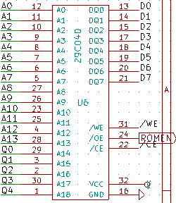
Finally we have all the signals we need to use our ROM chip. We find a part of the address bus (A0 to A13, allowing to access the 16K of a ROM slot) and the complete data bus (D0 to D7). The ROM selection bits Q0 to Q4 are connected to the additional address pins on the chip, allowing to select the correct data for the ROM slot being accessed.
There are 3 more signals: CE which enable the chip, WE to trigger a write (connected to WR of the expansion port, unless the write switch is off), and OE which triggers reads from the chip and is simply wired to ROMEN from the expansion port.
